

Metrology & Wafer Inspection demand the highest precision optical components to ensure flawless detection and measurement critical for semiconductor manufacturing and quality control. By employing advanced thin-film coatings and specialized optical designs, these components deliver exceptional accuracy, stability, and reliability across complex inspection and alignment systems.
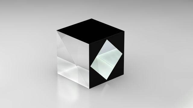
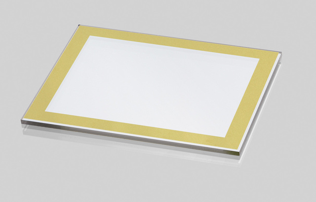
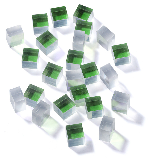
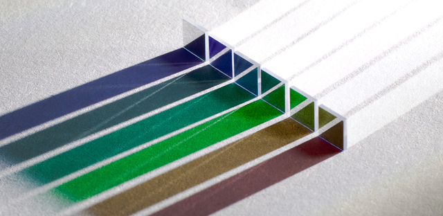
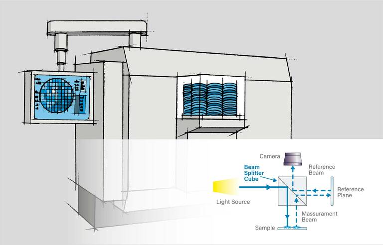
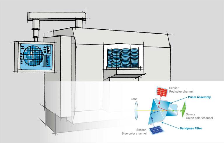
Materion’s optical coatings are engineered to meet the stringent requirements of metrology and wafer inspection equipment. Our portfolio includes conductive anti-reflection coatings, high-contrast beamsplitter cubes, and broadband mirrors designed to minimize stray light, suppress static discharges, and maintain stable performance over a wide spectral range. These coatings enable precise layer alignment, defect detection, and pattern inspection essential for maximizing yield and advancing chip design.
HIGH-PERFORMANCE OPTICAL COATINGS FOR METROLOGY SYSTEMS
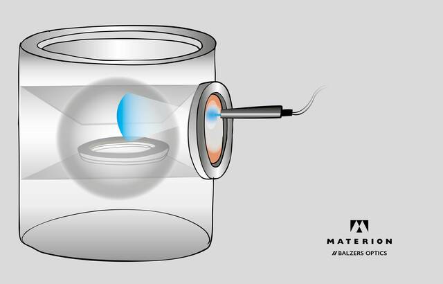
Our coatings provide excellent spectral uniformity and low reflectance, supporting overlay metrology systems that measure layer misalignments with nanometer accuracy. Materion’s expertise in Ion Assisted Deposition (IAD) and Ion Beam Sputtering (IBS) ensures coatings with high environmental stability and minimal ghost images, critical for reliable and repeatable measurements in semiconductor fabs.
ADVANCED SOLUTIONS FOR STATIC DISCHARGE PROTECTION
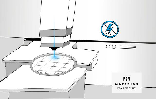
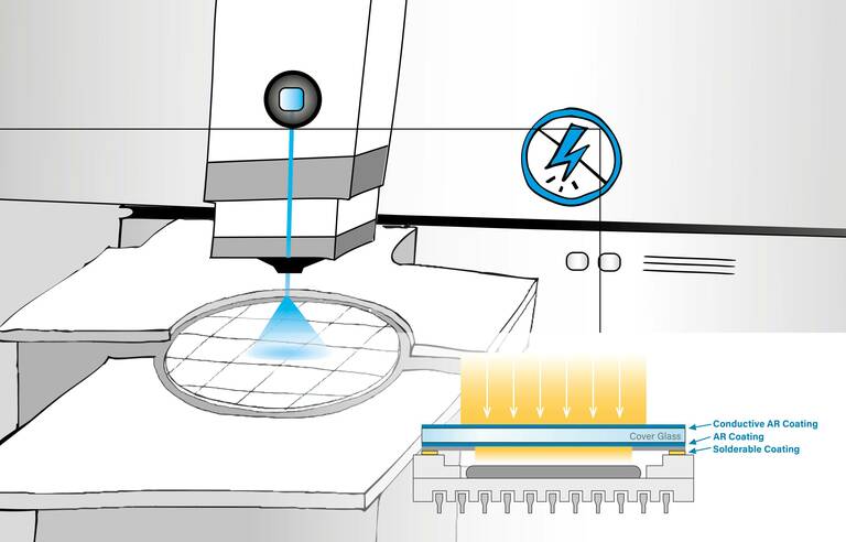
Materion’s conductive anti-reflection coatings reduce reflections and simultaneously prevent static discharges that can damage sensitive semiconductor substrates. This dual functionality protects wafer surfaces while enhancing optical signal quality, contributing to improved inspection accuracy and device reliability.
TAILORED OPTICAL COMPONENTS FOR DEFECT INSPECTION
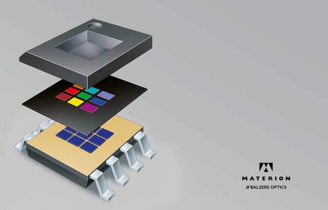
From detecting microscopic particles to identifying pattern misalignments and surface anomalies, our coatings support high-contrast imaging and precise light management. These solutions enable wafer inspection systems to identify defects early in the manufacturing process, boosting yields and pushing the boundaries of semiconductor technology.
CUSTOMIZED, HIGH-STABILITY OPTICAL COMPONENTS
Working closely with equipment manufacturers, Materion develops customized coatings tailored to specific wavelength, environmental, and performance needs. Our manufacturing processes ensure long-term coating durability and consistent optical properties, even in the demanding conditions of semiconductor production, supporting the ongoing evolution of metrology and wafer inspection technologies.
Benefits
- Precise, uniform coatings for accurate measurements
- Anti-reflection and static discharge protection
- Low stray light and high-contrast imaging
- Stable performance across broad wavelengths
- Enhanced defect detection and alignment
- Custom coatings for specific needs
- Durable for demanding semiconductor environments
Applications
- Overlay metrology for layer alignment
- Defect detection and pattern inspection
- Static discharge protection in semiconductor fabs
- High-contrast imaging systems
- Lithography process monitoring
- Precision optical measurement tools