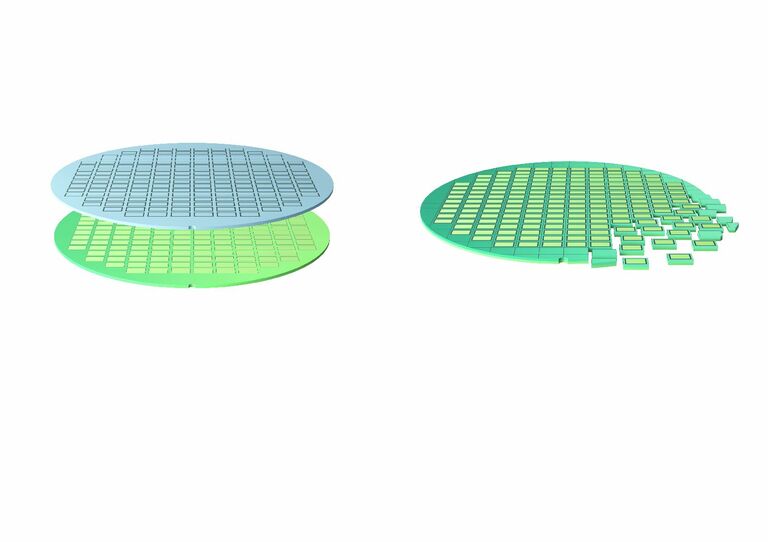
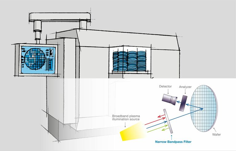


Wafers are foundational substrates in the production of high-precision optical components, enabling uniform, scalable fabrication of micro- and nano-structured surfaces essential for photonics, sensing, imaging, and display technologies. Materion Balzers Optics delivers wafers with exceptional material quality, surface flatness, and coating compatibility to support next-generation optical device performance and reliability.
Materion offers a comprehensive range of wafer solutions designed for superior uniformity, durability, and process integration.
High-Quality Optical Wafers
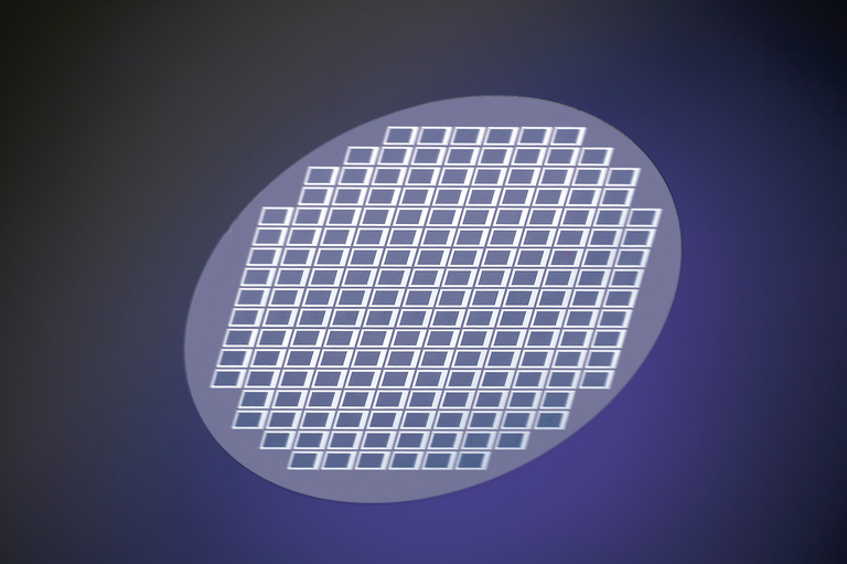
Our wafers feature ultra-flat surfaces with low roughness and tight thickness tolerances, supporting advanced lithography, coating, and patterning processes. Available in various substrate materials including fused silica, silicon, and specialty glasses, these wafers provide the ideal platform for precision optical fabrication.
Coated Wafers
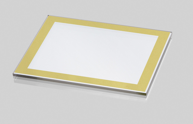
Leveraging Materion’s expertise in thin-film deposition, we offer wafers pre-coated with high-performance optical films such as anti-reflective coatings, dielectric mirrors, and filter stacks. These coatings are optimized for uniformity, adhesion, and environmental stability, enabling enhanced device functionality and longevity.
Pattern-Ready Wafers
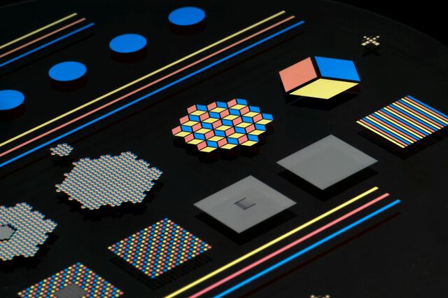
Materion supplies wafers engineered for seamless integration with advanced patterning techniques, including plasma-assisted reactive magnetron sputtering (PARMS) and photolithography. These wafers facilitate the creation of complex micro- and nano-scale optical structures with high accuracy and low defect density.
Custom Wafer Solutions
We collaborate closely with customers to provide wafers tailored to specific optical requirements, including custom sizes, materials, coatings, and surface treatments. This flexibility supports diverse applications from hyperspectral imaging to semiconductor photonics and wearable optics.
Benefits
- Ultra-flat surfaces with tight thickness tolerances
- High material purity and uniformity
- Compatible with advanced coating and patterning
- Excellent adhesion for thin films
- Low defect density for reliable performance
- Custom sizes and materials available
- Durable under varied environmental conditions
- Supports complex micro- and nano-structuring
- Enables scalable, repeatable manufacturing
- Ideal for diverse optical applications
Applications
- Hyperspectral and multispectral imaging
- Semiconductor devices
- Microdisplays and projection systems
- Wearable optics
- Precision calibration targets
- Advanced coating and filter fabrication